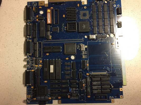
GBA1000 rev4 Build Log

Just a wild guess, but have you tried changing the position of jumper S5? I seem to remember having to fiddle with S5 and S7 to get my Fast RAM working, but that might have just been a 24-bit/32-bit mode thing.

IIRR the 32 bit mode is enabled by the flash rom, i don't think it's possible to totally disable the fast ram?


Sent from my iPhone using Tapatalk
 
IIRR the 32 bit mode is enabled by the flash rom, i don't think it's possible to totally disable the fast ram?

I was just thinking it may be possible to move the Fast RAM into the 32-bit address space but not have the flash either enabled or programmed so the RAM wouldn't be seen. Again, just a wild stab in the dark since I had no better ideas!
 
Thanks for your input guys. Yes, the S5 jumper is for activating the flash boot code so that the fastram is placed in 32bit. I haven't programmed the flash yet, but it's soldered. That should mean the 8MB shows up as 24bit I guess. Anyway, I tried with S5 in both positions and no luck.

The S7 is for the Zorro I think. It should be closed if not zorro-card is inserted according to the manual. I tried it in both positions but no difference.

EDIT: I also tested the GALs involved with the RAM (IC53-IC56) and they verified OK.
 
Last edited:
If the flashrom is not programmed, you can disable the fast ram activating the bootrom. In this case, the ram will not be attached to the system automatically.

So, flashrom empty and activated (S5 closed), you can test each fast memory Bank with the command addmem.

In practice, it's better to solder the first Bank and test it with addmem, if ok do the same with the 2nd, the 3rd and the 4th.

$1200000 - $13FFFFF (IC62, IC63, IC64, IC65)
$1400000 - $15FFFFF (IC66, IC67, IC68, IC69)
$1600000 - $17FFFFF (IC70, IC71, IC72, IC73)
$1800000 - $19FFFFF (IC74, IC75, IC76, IC77)

Just boot with no startup sequence and check for exemple Bank 0 :

addmem $1200000 $13FFFFF checkmem

It takes a little time and it should not give an error and the 1st bank (2MB Fastram) should be attached to the system.
If addmem return an error, you have to check eventually all solder joins.

With KS3.1 it's better to use a 3.1 Workbench.... Why mixing it with a WB2.0 ??
 
Last edited:
Many thanks gseb for your reply! This is exactly what I need to proceed, you have given me hope! Too bad I did not have this knowledge before I soldered all of those static RAMs. :)

Is it possible to use your approach with no flashrom soldered, but with S5 closed? I'm not sure if it was soldered properly, beacuse I could not program it using the GB_A1k_8MB_RAM utility. Will check for solder bridges and bad contact, but maybe I will have to remove it.

The reason for using WB2.0 was simply that I did not have any WB3-disk available.
 
I just got round to building a board and now starting on bringup/diagnostics. Unfortunately I don't have much in the way of the video circuit or 15KHz monitor so am trying the route of Indivision ECS (in the Denise socket) with a VGA to HDMI converter. Has anybody tried such a combination?

The ispLSI and GALs were programmed with my own hardware from a Raspberry Pi and cross-checked with a TL866 (seems to read and erase just fine, write questionable) so I'm somewhat confident for those (!). All are populated but I think only IC14 and IC57 are required for minimal testing?

Kickstart is DiagROM on a GGLabs F2R16 but I also have a 2.04 available. Chip RAM is Hitachi HM514400CS6 and no fast RAM fitted.

Jumpers: S1,S2 (closed) S3 (open with R128 ) S4,S5,S6,S7,S8 (open) X4 (down) X7 (N/A?) X16 (right) X21 (left)

The clock is a 40MHz crystal (no divider, so R122) feeding an MC68EC030RP40C. The signal and /HALT and /RESET (and /DTACK) lines I believe are operational but my Saleae only goes to 100MS so there's a lot of glitching between 33.3 and 50MHz due to its limited range; Perhaps there are some good lines I should measure in the 7MHz part of the circuit?

Reading this thread I get the impression the Agnus is probably most important after the ispLSI, for that I'm using a NOS 318069-18 sourced in the US; is that a known-good part or should I try a different 2MB PAL Agnus? Gary is a 318072-01, Paula 252127-02, Denise an OCS 8362R8; all of which believed NOS so untested.

Hopefully I can get hold of my A500+ soon to start swapping and testing parts to eliminate some of these variables..
 
in my first gba1000 i have mount a fatagnus standard 8375 and only cf-hdd not work, but i have sale (with zorro2-ide) and don't verify the fat-agnus code (i suppose 318069-11)

my second gba1000 are unpopulted
 
Thanks, I measured all of the IO signals for Agnus and ispLSI ICs (on a single channel so I could get 100MHz digital bandwidth and 10MS/s analog) and for the most part they look as expected for a system idling/just out of reset.

One thing that caught my eye was a lack of 7MHz clock on pin 38 (or 37 for that matter) of Agnus, both hovering around 3.9V. There is a 28MHz (NTSC XO) clock going into pin 34 and /XCLKEN (pin 36) is 4.8V (i.e. disabling an alternative external clock source on pin 35 which is multiplexed with A20, I think) so my guess is I need to try a new Agnus.

I have a PAL reference clock somewhere but I don't think this would cause such an issue.
 
In my effort to finish unfinished projects, I finally put together the second board I got in the kipper2k production run many years ago :) It didn't want to boot at first, and essentially there were two main problems:

1) some of the GAL chips were duds; they seemed to program fine but just did not work when installed in the motherboard
2) it's incredibly easy to get a little solder bridge somewhere under the fast RAM joints and not notice it, even though you have looked

I had the good fortune of having my earlier build (itself troubleshot by hese to have similar problems) to compare with, so it didn't take too long to figure out the issues. Everything works now and here's the final product:

gba1000_1.jpg


gba1000_2.jpg
 
Nice work!

How long does it take to solder in all the components?
 
@protek

It's hard to say, I did it over several days a little bit at a time. A lot of it has to do with the hassle of dealing with so many different components and keeping everything sorted out. I'd say that if you have a good space to work in, all the components nicely organized (so you don't have to search for things) and so on, one weekend is enough to complete a board.
 
I have bought a blank PCB rev 4. I broke out my microscope and soldering rig. Let's see if I can still solder and build stuff! With that being said, I have some questions that I hope someone can answer.

1. Is there anyone left that can either program all my chips or sell me programmed chips? Is there a link to the files that need to be programmed and is there a preferred programmer?
2. I am thinking of running a 3.1 ROM. Will that work or should I stick the 2.04 ROM?
3. Do I need to run a A1000 PS or will an ATX one work? I have read that you can convert an ATX PS but what I want is opinion. Is it a good idea and will it work?

I am sure that I will have more questions. Thanks to everyone for putting this thread together.
 
The GALs can be programmed with all manner of inexpensive programmers so they should not be a problem. Similarly there are lots of Lattice ISP programmers (or clones of them) available on eBay, although I can't recommend any one in particular as I didn't program the ispLSI1024 myself (didn't have a suitable adapter and couldn't be bothered to make one :)) I'm sure there are also people in the US who have built these and already have the programmers.

3.1 works fine, that's what I'm running in mine.

I elected to use an A1000 PSU since it's the best fit for the A1000 case. But pretty much any PSU can work, there is a jumper on the board for the Tick signal which is only present in the original PSU.
 
I bought most of my parts from the Mouser parts list the one of you fine gentlemen posted. I have a question about one of the parts. I ordered qty 100 of 623-2512067007Y3. This part is coming up as a 70 ohm 3A FB 1206 package. It looks like this was ordered for the 150 ohm FB that goes in multiple locations. Will this part work or should I order an actual 150ohm FB?

https://www.mouser.com/ProductDetail/Fair-Rite/2512067007Y3/?qs=P8bU7i9nNAWgDrI9bthl5Q==

The project also listed qty 6 of 810-ACH32C-100-T. Where do these go? I cannot locate them on any build sheet. Mistake in the project lsit on mouser??

Thanks!
 
Last edited:
Does anyone have part numbers for R26, C59, C80, and Q1?
R26 - 1K Trimmer Pot 4 pole
C59 - 1-5 pF Trimmer 3 pole
C80 - 5-40 pF Trimmer 3 pole
Q1 - 32Khz Oscillator for the RTC. 2 pole.

Thanks!
 
I am almost ready to fire this beast up. I just finished soldering the 16 ram chips onto the board. Its looking sexy!!

I have figured out how to program my GAL chips. The issue now is the lattice. I can make the adapter but my MiniPro programming software does not have a template for this chip. Anyone have a recommendation of what software or what template to use for programming the lattice chip?

Anyone?
 
Last edited:
Hi Icepick, where did you get the missing parts ?

I am also searching for the sockel PGA128
 
Back
Top Bottom