You are using an out of date browser. It may not display this or other websites correctly.
You should upgrade or use an alternative browser.
You should upgrade or use an alternative browser.
Building a new Super C64 PSU
- Thread starter BloodyCactus
- Start date
- Replies 28
- Views 6313
BloodyCactus
Member
Just need some chips to come from Mouser, apparently will be here on Wedneday. Hopefully this weekend I can start the physical build now!

specialK
New member
This is very interesting project, I wish you were making extra for sale... And another version for Atari XE ")
Sent from my iPhone using Tapatalk
Sent from my iPhone using Tapatalk
BloodyCactus
Member
so ages pass, and come again and we throw out the old design and whip up a new design.

so now to find time to test it and get back on this project!
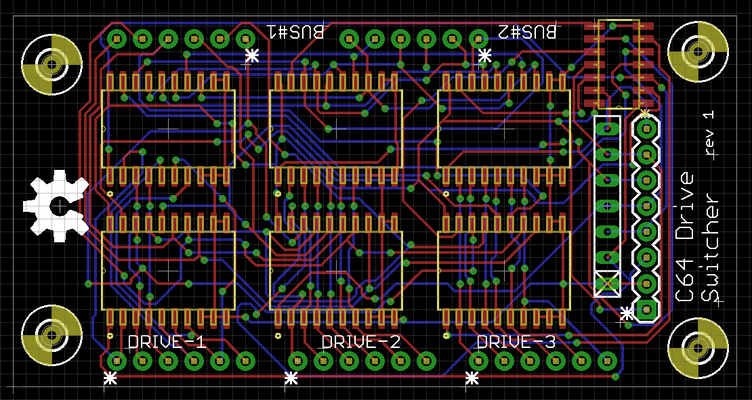
A little explanation since this board is kinda brefit of silk screen id's.
bottom row of 4x 5pin headers are the 4 input IEC drives. the side 2x 5pin headers are the two busses (c64#1,c64#2 or c128 etc).
The top row is the 4 input toggle switches that direct a drive to a bus, and some power helper pins for the front panel.
sooo... I kept talking about 5 pin headers but the IEC bus has 6 pins... well, the chips I am using switch 4 pins (the 5th pin is ground)....
The IEC bus is 5 pins if you remove ground... but I can only switch 4. So my choice is, do I switch do VIC20 compatability? (RESET pin) or C128 compat (Serial SRQ)..
since I dont have a vic20 I am going to ignore the reset pin and switch pins 1,3,4,5. I dont actually know how well this will work so, we will see.. well I know reset is somewhat required so it may be I keep reset and ignore SRQ but then no 1571 external drive or 1581 (which would not matter on c64...) argh decisions.
[TABLE="class: cms_table"]
[TR]
[TH="align: center"]Pin[/TH]
[TH="align: center"]Description[/TH]
[TH="align: center"]Signal direction[/TH]
[TH="align: center"]Remark[/TH]
[/TR]
[TR]
[TD="align: center"]1[/TD]
[TD]SERIAL SRQ[/TD]
[TD]IN[/TD]
[TD]Serial Service Request In, at the C128 "Fast Serial Clock"[/TD]
[/TR]
[TR]
[TD="align: center"]2[/TD]
[TD]GND[/TD]
[TD]-[/TD]
[TD]Ground, signal ground (0V)[/TD]
[/TR]
[TR]
[TD="align: center"]3[/TD]
[TD]SERIAL ATN[/TD]
[TD]OUT[/TD]
[TD]Attention, for the selection of a device at beginning/end of a transmission[/TD]
[/TR]
[TR]
[TD="align: center"]4[/TD]
[TD]SERIAL CLK[/TD]
[TD]IN/OUT[/TD]
[TD]Clock (for data transmission)[/TD]
[/TR]
[TR]
[TD="align: center"]5[/TD]
[TD]SERIAL DATA[/TD]
[TD]IN/OUT[/TD]
[TD]Data[/TD]
[/TR]
[TR]
[TD="align: center"]6[/TD]
[TD]SERIAL RESET[/TD]
[TD]OUT(/IN)[/TD]
[TD]Reset, in older VIC-20 unused
[/TD]
[/TR]
[/TABLE]
so now to find time to test it and get back on this project!
A little explanation since this board is kinda brefit of silk screen id's.
bottom row of 4x 5pin headers are the 4 input IEC drives. the side 2x 5pin headers are the two busses (c64#1,c64#2 or c128 etc).
The top row is the 4 input toggle switches that direct a drive to a bus, and some power helper pins for the front panel.
sooo... I kept talking about 5 pin headers but the IEC bus has 6 pins... well, the chips I am using switch 4 pins (the 5th pin is ground)....
The IEC bus is 5 pins if you remove ground... but I can only switch 4. So my choice is, do I switch do VIC20 compatability? (RESET pin) or C128 compat (Serial SRQ)..
since I dont have a vic20 I am going to ignore the reset pin and switch pins 1,3,4,5. I dont actually know how well this will work
so, we will see.. well I know reset is somewhat required so it may be I keep reset and ignore SRQ but then no 1571 external drive or 1581 (which would not matter on c64...) argh decisions.[TABLE="class: cms_table"]
[TR]
[TH="align: center"]Pin[/TH]
[TH="align: center"]Description[/TH]
[TH="align: center"]Signal direction[/TH]
[TH="align: center"]Remark[/TH]
[/TR]
[TR]
[TD="align: center"]1[/TD]
[TD]SERIAL SRQ[/TD]
[TD]IN[/TD]
[TD]Serial Service Request In, at the C128 "Fast Serial Clock"[/TD]
[/TR]
[TR]
[TD="align: center"]2[/TD]
[TD]GND[/TD]
[TD]-[/TD]
[TD]Ground, signal ground (0V)[/TD]
[/TR]
[TR]
[TD="align: center"]3[/TD]
[TD]SERIAL ATN[/TD]
[TD]OUT[/TD]
[TD]Attention, for the selection of a device at beginning/end of a transmission[/TD]
[/TR]
[TR]
[TD="align: center"]4[/TD]
[TD]SERIAL CLK[/TD]
[TD]IN/OUT[/TD]
[TD]Clock (for data transmission)[/TD]
[/TR]
[TR]
[TD="align: center"]5[/TD]
[TD]SERIAL DATA[/TD]
[TD]IN/OUT[/TD]
[TD]Data[/TD]
[/TR]
[TR]
[TD="align: center"]6[/TD]
[TD]SERIAL RESET[/TD]
[TD]OUT(/IN)[/TD]
[TD]Reset, in older VIC-20 unused
[/TD]
[/TR]
[/TABLE]
SkydivinGirl
Retro Girl
Looking good. Does the IEC switch allow you to switch between multiple drives for a single C64 or does it allow you to share drives with multiple C64s?
Heather
Heather
BloodyCactus
Member
the idea is to let you toggle switch which drive is connected to which c64. so if you had 2 c64's you could toggle which drive was connected to which c64. the downside is, drive id#'s are hardcoded on the hardware so switching two drive #8's etc but I could easily toggle my uIEC/SD between c64's.
the '5th pin' that I dont bus is driving me crazy.. thinking of doubling the chip count just so I can get all the signals in. arggh. then I would not have to worry about vic20 or c128 compatability.
but I could easily toggle my uIEC/SD between c64's.the '5th pin' that I dont bus is driving me crazy.. thinking of doubling the chip count just so I can get all the signals in. arggh. then I would not have to worry about vic20 or c128 compatability.
SkydivinGirl
Retro Girl
The QuadPortIEC will let you enable and disable IEC devices but it will not let you use a single IEC device on multiple C= systems. I know there are a lot of people, including me, who would like that functionality. ")
Heather
Heather
BloodyCactus
Member
The QuadPortIEC will let you enable and disable IEC devices but it will not let you use a single IEC device on multiple C= systems. I know there are a lot of people, including me, who would like that functionality.
Heather
hmm Ive never seen that quadportiec before.
I dont think you can use a single iec device on multiple c= systems because of how the bus works and how its driven by the c64.
SkydivinGirl
Retro Girl
There was a device made that would allow multiple computers to share a single floppy drive. Jim Brain has done some work on creating a new version of that but I can't remember what the original device was called.
Heather
Heather