Suggestions for floppy issue in A600...

  • Thread starter Thread starter mfilos
  • Start date Start date
  • Replies Replies 34
  • Views Views 14347
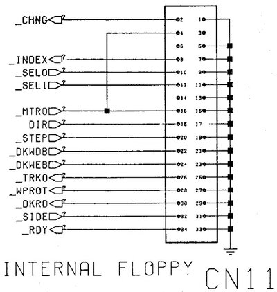
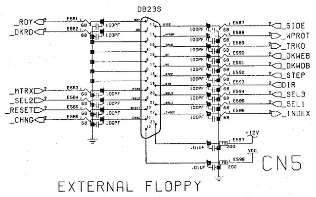
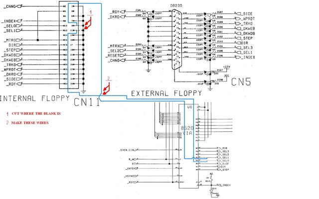
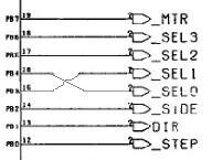
Mario, i don't know if you intend to boot from an external floppy, but have a look here too: http://www.amigahistory.co.uk/hardwarefaq.html

Q. How can I persuade the OS that my second floppy drive is DF0: as my internal drive is damaged?

A. You could use a tool like Degrader, which allows floppy drives to be remapped to others as well as disabled. Otherwise add the following to your S:User-Startup:

; Disable DF0: and map DF1: in its place
Assign Dismount DF0:
Assign DF0: DF1:

This will fool any CLI commands, so you can CD to DF0: and DF1:, reaching the same destination drive. Even DMS works with this system. However most games and demos will use custom / non OS-legal floppy addressing and will fail.

Might come in handy if/when you find an external unit...
 
Thanks Salaxi I knew about that solution while googling today... I don't want software but hardware solution since I want full compatibility.
 
Well that means that you need to be able to boot off it too then...
I guess there's a solution, but we can only dream of making it possible: The Shuffle Board! http://amiga.resource.cx/exp/shuffle
But that would be like Science Fiction due to:
a) most probably uber-rare item,
b) a hell of a hack to try adapting it to the A600's chipset... :)
 
As said before, that's a simple question of cutting the two tracks (SEL0 & SEL1) and cross the lines, where SEL0"in" goes to SEL1"out" and vice versa.

A good spot is the floppy header and the External drive socket (internally).
 
From A600's schematic (see below pictures) I see that in C11 (floppy header):
- Pin 10 = SEL0
- Pin 12 = SEL1

In C5 (External floppy connector):
- I don't see a SEL0 pin
- Pin 21 = SEL1

And lastly in U8 (internal floppy controller):
- Pin 16 (PB3) = SEL0
- Pin 16 (PB4) = SEL1

Sorry but I don't get it :nuts:

Can you be more specific please?
 

Attachments

  • cn11.jpg
    cn11.jpg
    49.4 KB · Views: 5
  • cn5.jpg
    cn5.jpg
    79.3 KB · Views: 8
  • u8.jpg
    u8.jpg
    41.2 KB · Views: 5
My understanding is portrayed in the following attachments:

Only thing i changed are the traces to pins 15 and 16 instead of 13 and 14 on U8 to correspond to the proper signals..
 

Attachments

  • Z's way.JPG
    Z's way.JPG
    179.5 KB · Views: 6
  • cross.JPG
    cross.JPG
    7.2 KB · Views: 3
Yes that is what I thought also but isn't Pin 9 and Pin 11 the ground? SEL0 and SEL1 are Pin 10 and pin 12... :wooha:

Also... how the hell does the numbering start on U8? There's a no.1 on the right side but what does it mean? Center of right side clockwise?... Oh well

Editing the photo (like Salaxi did on schematics) with info of where to cut trace and where to solder would help tons!!!
This photo was from BBOAH, i'll put a higher resolution one once i'll go home in case it's needed
 

Attachments

  • C11-U8.jpg
    C11-U8.jpg
    143.6 KB · Views: 8
I'll use a "cheap" way to solve your problem:

-Cut the internal "leg" SEL1 (pin #21) of the external floppy connector. Keep it "flying" for now;

- Using a wire jumper (better with a wire with a proper connector), route the SEL0 signal from the floppy header to the now "flying" leg. Solder the wire in the leg.

-Don't bother with the SEL1 signal, you'll never see it again.

-Done.
 
I think that this is a nice approach my friend! Thanks!
I'm gonna try it as soon as I have an external floppy soon :)
Cheers my friend

P.S. What about the waiting part (searching for floppy) in case external floppy isn't mounted?
Can we also make a hack with a diode shortening like the DF0 Internal header hack?
 
I just found an interesting chart with the pinouts, dunno if anyone is familiar with it.. http://www.amiga-stuff.com/hardware/8520.html

U7 (CIA-A), U8 (CIA-B)PLCC1 MHz or 2 MHz

If you go down about mid-page, you'll notice a label saying: PLCC package pinout for Amiga use
That's where the pinout is!

EDIT: OK, i got your thinking, it's not the pinout you're worried about, it's the orientation.. :-)
The "1" mark which you refer to, is next to the right-side middle of U8. These are 44-pin PLCCs, just about standard in most cases. Next to the white "1" close to the edge of the chip there should be a tiny inward "crater" LOL (can't really come up with the correct terminology). Pin 1 is the 6th pin at that side, no matter if you start counting from the left or the right corner, since there's 11 pins on each side. But going towards the upper right "diagonal" corner (the only one like that) you reach pin 6. Phew, that was some Greek talk ing there, eh? haha
Anyway, to simplify things a bit, here's an example: http://www.controlchips.com/manuals/cy545/545-02c.htm
Don't pay attention to the signals there, but the pin numbering!
Here's another example: http://wapedia.mobi/en/File:KL_Intel_80C88.jpg You can clearly see the dot there..
http://www.datasheetcatalog.org/datasheet/intersil/fn2949.pdf' (Numbering goes the same way, counter-clockwise)
 
Last edited:
Salaxi mate thanks for these info. They helped a lot :)

Rkauer/Zetr0 my friends, now that I saw it closely and buzzed Pin 21 of the external connector (internal) it seams that the pin is not the one visible but the one underneath mobo, so it's kinda difficult to cut and wire...

On the other hand I saw the previous Zetr0/Rkauer approach and it seems pretty easy after I read it some more times. If I got it correctly I need to do the following only:

Check the picture that I edited bellow
- In Yellow it's the trace cutting
- In Red are the new wires that need to be attached to both CN11 and U8


What do u think? Am I right?
 

Attachments

  • C11-U8.jpg
    C11-U8.jpg
    135.4 KB · Views: 11
Cutting and crossing the lines near the CIA chip will suffice.
 
hi guys giving life to this thread now we have write support for hxc can it be used as df0 from external drive pluged in back
 
Salaxi mate thanks for these info. They helped a lot :)

Rkauer/Zetr0 my friends, now that I saw it closely and buzzed Pin 21 of the external connector (internal) it seams that the pin is not the one visible but the one underneath mobo, so it's kinda difficult to cut and wire...

On the other hand I saw the previous Zetr0/Rkauer approach and it seems pretty easy after I read it some more times. If I got it correctly I need to do the following only:

Check the picture that I edited bellow
- In Yellow it's the trace cutting
- In Red are the new wires that need to be attached to both CN11 and U8


What do u think? Am I right?

Hi!

Let me resurrect this thread after years.

I have done this mod on 2 Amigas 600.

First one - external Gotek (jumper SD0) is seen as DF0:. Internal drive is "dead". Is it as it should be?


Second one - problems. external Gotek (jumper SD0) is seen as DF0:, but not completely. When I disconnect internal FDD, it boots from Gotek, but some programs and games stop while loading and Workbench screen appears asking me to replace volume ABC in any drive. All Workbench disks behave like that.
When I connect both Gotek and internal FDD, it kind of messes up the system, they are both seen as one drive, eg. I have a Wotkbench ADF in gotek and some game floppy in internal, it boots form internal and then asks me to replace a Worbench floppy.
When I set Gotek jumper to SD1, I can load everything (games etc. - behaves like df0: ) without the requests to replace, but it is seen as DF2:, and internal probably as DF0:. There is also some conflict of drives when both are connected like that, but i don't remember exactly.

To sum up, external Gotek only runs properly with with jumper set to D1) when internal FDD is disconnected, it behaves like DF0:, but is seen as DF2:.

Where have I screwed up?

Thanks!

EDIT: When only internal is connected, it works as DF0 normally.
 
Last edited:
I have done this mod on 2 Amigas 600.

First one - external Gotek (jumper SD0) is seen as DF0:. Internal drive is "dead". Is it as it should be?

Yes.

Second one - problems

If you have performed the mod EXACTLY as on the first A600, then there should be no difference in behaviour at all.
Maybe some trace hasn't been perfectly cut and still conducts, or some imperfect soldering has caused a short. Closely examine the mod.
 
Last edited:
Back
Top Bottom