Picture shows model with castellated half-holes, and 1M x 4 dram. (There are some new pcb:s with normal holes.)

4 pcs 15€, 5 pcs 17€ (1 spare if fragile castellated hole breaks), shipping 2.75€.
50 pcs 100€ + registered mail shipping 22/27 € Europe/World (includes tracking except for Australia, possibly other countries)
- also can be sold with soldered on round, or square
pin (7.5mm) headers, lower profile "white type", as well as the more common black ones with thinner and longer pins (check if there is not enough space under A500 keyboard for either of these pin headers + socket) - 4 pcs 20€


New versions: Up to 30 pcs adapters with lower capacity 256K x 4 SOJ DRAM , and 20 pcs with 1M x 4 TSOP DRAM. These have regular holes instead of castellated half holes. Price the same (4 pcs 15€ without pins, 20€ with pins)

Install
Can be soldered to board (Using kapton tape for insulation, use conical tip perhaps, use flux, clean flux to see joints in good light, joints can inspected using magnifying loupe. Suspect joints should be fixed. The castellated half holes made in the original pcb lot are not great, at least one broke off during soldering. I am offering spares for sale.
Also round pin headers can be used for insertion to socket, but there is no much space for it in A500 under the keyboard.
The original lot has 1M x 4 DRAMs, it can be configured for 256K x 4 use by grounding MA9 of the DRAM, assuming the DRAM doesn't mind 3/4 of it not being refreshed or accessed. This address line can also be connected to DIP pin 5 with the SMD solder blob jumper, maybe for other uses than Amiga, which connects pin 5 to pin 4 (other /RAS) of every other dram.
More "info":
The boards have some of the address lines "shuffled", but I don't think it's problem with simple random access memory. E.g. refresh by ram controller going from location 0 to max won't go in fully successive order on the chip, but so what?
Here's the old thread where 2 megs of on board chip ram is created for A500+ MB that had originally only 512K (the kind of board that was used inside amiga that was sold as regular A500 with ks1.3?).

 www.amibay.com

Combining *RAS0 and 1 signals can be done with and gate, which is "or" function for active low signals.
A two schottky diode "wire or" for combining active low ras signals can have quite high low-level voltage, around 0.6V and noisy. (max. low level for a ttl-level input 0.8V), measured after the 180 ohm pull up was moved right to the diode anodes and also the signal was moved through a 68 ohm series termination forwards, and at the end of line being the original 4.7 kohm pull-up.
BAT54A common anode dual schottky could be soldered to JP3 pads. If i had a BAT54A and the pads, they were accidentally pulled off.
I tried an 74AHCT2G08 and-gate with 0.5mm pitch . The signal was slow-wavy at the other end. Unfortunately one wire came loose when I was gluing it all in place.

So I put in a DIP 74F08.

1M x 4 dram HM514400 takes refresh address from ma0..ma9. Amiga 500(+) normally uses drams with ma0..8.

Checking that 8375 Agnus toggles MA9 in refresh cycles where both /ras signals go active low. Then 74HCT02 creates trigger for oscilloscope, blue signal.

MA9 is both low and high at different refresh cycles.
4 pcs 15€, 5 pcs 17€ (1 spare if fragile castellated hole breaks), shipping 2.75€.
50 pcs 100€ + registered mail shipping 22/27 € Europe/World (includes tracking except for Australia, possibly other countries)
- also can be sold with soldered on round, or square
pin (7.5mm) headers, lower profile "white type", as well as the more common black ones with thinner and longer pins (check if there is not enough space under A500 keyboard for either of these pin headers + socket) - 4 pcs 20€
New versions: Up to 30 pcs adapters with lower capacity 256K x 4 SOJ DRAM , and 20 pcs with 1M x 4 TSOP DRAM. These have regular holes instead of castellated half holes. Price the same (4 pcs 15€ without pins, 20€ with pins)
Install
Can be soldered to board (Using kapton tape for insulation, use conical tip perhaps, use flux, clean flux to see joints in good light, joints can inspected using magnifying loupe. Suspect joints should be fixed. The castellated half holes made in the original pcb lot are not great, at least one broke off during soldering. I am offering spares for sale.
Also round pin headers can be used for insertion to socket, but there is no much space for it in A500 under the keyboard.
The original lot has 1M x 4 DRAMs, it can be configured for 256K x 4 use by grounding MA9 of the DRAM, assuming the DRAM doesn't mind 3/4 of it not being refreshed or accessed. This address line can also be connected to DIP pin 5 with the SMD solder blob jumper, maybe for other uses than Amiga, which connects pin 5 to pin 4 (other /RAS) of every other dram.
More "info":
The boards have some of the address lines "shuffled", but I don't think it's problem with simple random access memory. E.g. refresh by ram controller going from location 0 to max won't go in fully successive order on the chip, but so what?
Here's the old thread where 2 megs of on board chip ram is created for A500+ MB that had originally only 512K (the kind of board that was used inside amiga that was sold as regular A500 with ks1.3?).
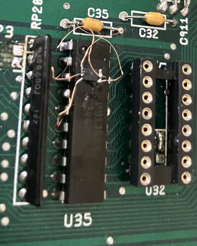
SOJ RAM to DIP-20 footprint adapters with 1M x 4 drams
4 pcs 15€, 5 pcs 17€, shipping 2€ Can be soldered to board (kapton tape for insulation, conical tip perhaps, flux, cleaned, joints inspected with loupe) One of the dram adapters in picture on socket after replacing one one board. Also for sale 74F139 0.75€/pce
Combining *RAS0 and 1 signals can be done with and gate, which is "or" function for active low signals.
A two schottky diode "wire or" for combining active low ras signals can have quite high low-level voltage, around 0.6V and noisy. (max. low level for a ttl-level input 0.8V), measured after the 180 ohm pull up was moved right to the diode anodes and also the signal was moved through a 68 ohm series termination forwards, and at the end of line being the original 4.7 kohm pull-up.
BAT54A common anode dual schottky could be soldered to JP3 pads. If i had a BAT54A and the pads, they were accidentally pulled off.
I tried an 74AHCT2G08 and-gate with 0.5mm pitch . The signal was slow-wavy at the other end. Unfortunately one wire came loose when I was gluing it all in place.
So I put in a DIP 74F08.
1M x 4 dram HM514400 takes refresh address from ma0..ma9. Amiga 500(+) normally uses drams with ma0..8.
Checking that 8375 Agnus toggles MA9 in refresh cycles where both /ras signals go active low. Then 74HCT02 creates trigger for oscilloscope, blue signal.
MA9 is both low and high at different refresh cycles.
Attachments
Last edited: